Array phase modulator based on optical phased array
Optical phased array technology realizes beam deflection and continuous scanning by controlling each coherent synthesis unit beam phase. It has the characteristics of no mechanical inertia, high scanning accuracy, and high resolution—a research hotspot in the military, space communication, and other fields in recent years. The phase modulator is the core device of laser phased array technology, which determines the deflection beam's quality and scanning accuracy. At present, the most commonly used phase modulator is a single waveguide phase modulator based on the electro-optic effect of lithium niobate crystal, which has the advantages of fast, flexible, and high precision. Huang et al. [3] of the Massachusetts Institute of Technology built a 7-channel laser phased array using the lithium niobate waveguide phase modulator produced by the EO space company, realizing fast and high-power beam scanning. However, the single-channel phase modulator increases the system's complexity and power loss, which is not conducive to the development of a large array laser phased array system.
Based on the principle of integrated optics and annealed proton exchange technology, an array phase modulator is designed and fabricated in this paper. The device integrates a one × four beam splitter and a 4-way phase modulator on a chip, which improves the system's integration.
1、Refractive index distribution of ape optical waveguide
Compared with Ti diffused waveguide, PE waveguide has many advantages, such as low diffusion temperature, high anti damage threshold, polarization selectivity, etc. Generally, lithium niobate crystal is used as the base material of proton exchange, and benzoic acid is used as the proton source. They react chemically at high temperatures to form a waveguide structure with the step-index distribution. After full annealing, the waveguide can realize the α single-crystal phase, which has a small waveguide index difference, good crystal structure integrity, and low transmission loss. The refractive index distribution of annealed ape strip waveguide [4-6] is as follows:

Where Δ n is the increment of the refractive index of the waveguide surface, Nb is the abnormal refractive index of the lithium niobate substrate, and f (x) and G (y) represent the refractive index distribution functions in the width direction and depth direction of the waveguide respectively.
Waveguide width direction, refractive index distribution is

Where: ERF is Gaussian error function; s = 2x / W, W is the width of waveguide mask opening; DX is the diffusion length in the width direction, which is related to annealing temperature and annealing time.
In the depth direction of the waveguide, the refractive index distribution is:

Where: G is the shape factor, usually 2; dy is the effective depth of the waveguide, which is also related to the annealing temperature and time.
The refractive index distribution of ape waveguide is determined by annealing temperature and time. Choosing the right temperature and time, we can make the needed high quality waveguide.
2、 design principle
2.1 Device principle
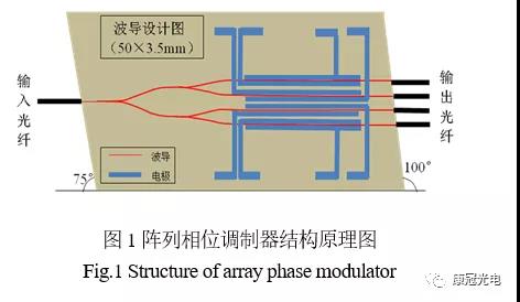
Figure 1 shows that the integrated array optical waveguide phase modulator integrates the beam splitting unit and phase control unit on a lithium niobate chip. The input and output are single-mode polarization-maintaining fibers. The beam splitting company adopts the cascade Y branch structure to achieve four uniform output channels; the phase control unit adopts the long electrode structure. The four pairs of electrodes are respectively led out from both sides of the chip. The chip's input and output are cut at 75 ° and 100 ° angles, respectively, to reduce the optical reflection between the optical fiber section and the waveguide section. The whole chip is about 50 mm long and 3.5 mm wide.
3、Device manufacturing and testing
3.1 Device fabrication
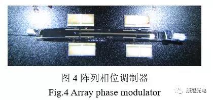
According to the above design principle, firstly, the waveguide layout and mask are made. In plate making, three groups of waveguides with different widths are made on each board. After photolithography, proton exchange, annealing, and other processes, each waveguide group is coupled with optical fiber and tested with light. A group of plating electrodes and packages with better optical characteristics are selected, and finally, the array phase modulator is obtained, as shown in Figure 4.
3.2 Parameter test
The device's optical characteristics mainly include insertion loss (I.L) and output uniformity (F.L). They are essential parameters to measure the performance of the device. The lower the insertion loss is, the higher the output uniformity is, the better the understanding of the device is.
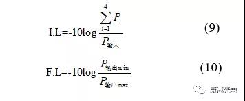
PI refers to the power of the ith output Max representing the minimum and maximum output ports' power.
The integrated waveguide phase modulation device was tested with a 1064nm light source and optical power meter. The test results are shown in Table 1. The results show that the device's output uniformity is good, and the insertion loss needs to be further reduced by optimizing the waveguide structure.

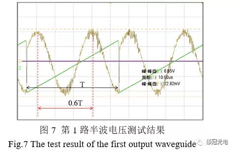
Half-wave voltage is an important parameter to measure the electrical characteristics of devices. The lower the half-wave voltage, the better the electrical parts of devices. In this paper, the half-wave voltage of the integrated device is measured using the principle of Mach Zehnder intensity modulation. The test schematic diagram is shown in Figure 5. Load sawtooth wave electric signal with saw period of T and peak value of VPP on one arm of Mach Zehnder intensity modulation system. Use a double trace oscilloscope to observe the output intensity signal. In theory, the output signal should be a sine signal with the cycle of T. compare it with the loaded sawtooth wave signal to get half-wave voltage:
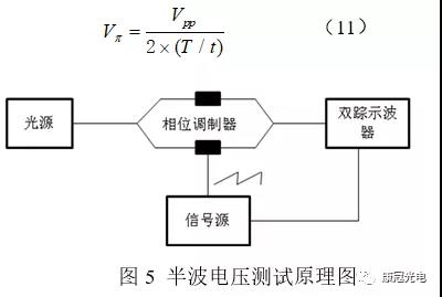
Fig.5 The schematic diagram of half-wave voltage test
In this paper, two array phase modulators are used to build a half wave voltage test system based on the principle of Mach Zehnder intensity modulation, as shown in Figure 6.
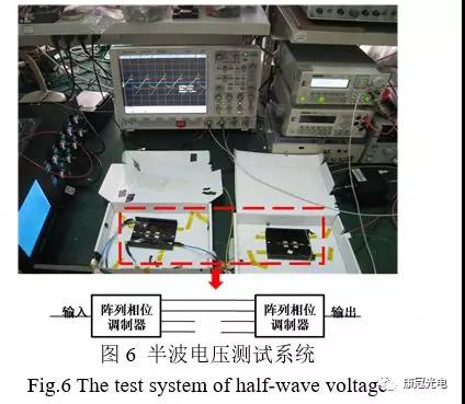
Firstly, the first and second channels are used to build the test system, and the first channel electrode is loaded with sawtooth wave signal with peak to peak value of 7V and frequency of 100kHz. The output signal tested by the oscilloscope is shown in Figure 7, and each sawtooth period includes. According to formula (11), the first half wave voltage is 2.1V. Similarly, the other three half wave voltages are tested, and the test results are shown in Table 2.
The test results show that the half wave voltage of the 1st, 3rd and 4th circuit is very consistent with the theoretical value. The third circuit electrode interrupts a gold wire (connecting the electrodes on both sides of the waveguide and the external electrode plate, and using two gold wires in the design), so the measured half wave voltage is higher than the theoretical value.


