Design flow of RF power amplifier
1. Device selection
Before the time-consuming tasks such as load and source traction, matching network-integrated design, and so on, we need to fully carry out the device/process selection to find the best candidate device that meets the specific criteria. Based on the frequency and power given by the device index for multiple candidate devices can be found. Other parameters such as CDs, CGS, and impedance conversion ratio are also considered in addition to the usual considerations such as working voltage VDS, gain, operating frequency, and rated power.
2. Extraction of optimal load impedance
Once the device is selected, and the corresponding nonlinear model is obtained, it is used to determine the optimal source impedance and load impedance. The load impedance, which can achieve the maximum power, efficiency, and gain, or achieve some desired tradeoff between these performances, varies with the frequency and will vary significantly within the working bandwidth of a broadband power amplifier. Through drawing the load traction diagram of fundamental frequency and harmonic frequency simultaneously in the microwave office software and using the waveform engineering method (circuit design technology based on shaping the transistor voltage and current waveform), the correct load impedance is determined.
The waveform engineering method relies on obtaining intrinsic nodes' information across the transistor current source reference plane rather than the information on the reference plane after packaging. Assuming that the nonlinear device model provides these nodes, the waveform engineering method can use the technique of human eye observation to analyze the voltage and current swing, clipping, and the type of amplifier operation.
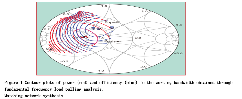
In the example of this article, the load pulling is carried out under the conditions of Vds= +28V and Idq=90mA, scanning the entire working frequency band and extracting the impedance for the best power and efficiency. The results in the middle of the frequency band are shown in Figure 1.Obviously, the larger this area is, the easier it is to design impedance matching. With the frequency sweep in the operating frequency band, Pmax in Figure 1 forms a compact and clockwise curved track beneficial to broadband amplifiers' design. The load pulling on the fundamental frequency is that the RF power amplifier's broadband characteristics make it challenging to achieve the best harmonic terminal load without introducing transmission zeros in the matching network. The bag pulling analysis was also carried out on the second harmonic, and a high-efficiency impedance region two that can be controlled in the network synthesis was found.
When designing a narrow-band RF power amplifier, the optimal load does not change much within the working frequency band, making the task of network design less complicated. not to say that matching low score bandwidth is always simple. The source and load impedance analysis shows that the network's fundamental frequency impedance must often be controlled to a single impedance point to achieve the high performance of the RF power amplifier. Once the network's impedance trajectory deviates from the target load impedance, it will bring excellent execution. Loss. The requirements for precise control of the harmonic terminal impedance in class F and F-1 amplifiers make the design task's complexity more than that of the ordinary class of power amplifiers.
In the design of broadband RF power amplifiers, especially to achieve higher performance indicators, the amplifier's matching network needs to control the fluctuation of its impedance under a much larger fractional bandwidth. After determining the best impedance and target area, the load matching network can use a simplified fundamental frequency technique (SRFT)3 to design an ideal lumped element network, convert it into a distributed step impedance form4, and then perform electromagnetic (EM) Simulation. In this article's example, the EM simulation results are in good agreement with the model predictions; however, for unconventional matching topologies, this may not be the case. EM simulation can be regarded as an essential step in reducing uncertainty in the design process.
One design technique is to use the conjugate impedance of the best impedance as the internal resistance of the signal source (port 1) at both ends so that the design of the matching network can be transformed into reducing the complex source impedance and the 50-ohm terminal load within the working bandwidth of the amplifier—the mismatch between the two leads to the problem of loss. You can evaluate the network's mismatch on the 50Ω side (port 2) of the network, as shown in Figure 2a. The output matching circuit is a passive network, so its operating power gain is less than one and equal to the efficiency caused only by internal dissipation losses. Since there is still reflection loss at the input end, the product of the loss and the corresponding efficiency of the internal dissipation is equal to the transmission power gain, and its value must be smaller. These quantities are plotted as percentages in Figure 2b. The calculated load network efficiency at the frequency of 2800MHz is 96.6%, close to the value calculated in the return loss at the same frequency. For further comparison, calculate the operating power gain considering only the pure ohmic loss in the network, and it can be seen that the computed efficiency is 97.7%. Although this calculation does not directly include the reflection loss, its value does vary with the terminal impedance. These impedances will affect the current and voltage distribution in the existing network, thereby affecting
the losses in copper and dielectrics, respectively.
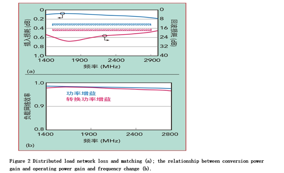
The conversion gain is evaluated by a signal source with an internal resistance conjugated to the target load impedance at the device's drain. Although the output end is matched according to the optimal conditions of power compression and efficiency, rather than the minimum reflection condition of the drain, it is found that the compression power reduction caused by the use of conjugate matching conditions and the non-ideal realization of the target load impedance The resulting decrease in compression power fits well. Therefore, the conversion power gain can be plotted as an effective means to evaluate output matching's overall effect.
Due to the following reasons, the optimal broadband matching achieved by using this transistor is relatively straightforward:
Achieving the best Pmax The load impedance area is more compact.
- The best impedance has a trajectory that rotates clockwise as the frequency increases.
According to the practical criterion of having a reasonably low impedance transformation ratio, GaN devices are the preferred device type for broadband RFPA.
Source matching network
The bandpass filter network can control the fluctuation of the source impedance in the entire working frequency band. Simultaneously, this method also has the advantage of reducing low-frequency gain and overcomes the problem of very high low-frequency intrinsic gain of the transistor. This specially designed source impedance matching network is also responsible for improving the low-frequency stability of the amplifier. Since the impedance transformation ratio of this network is 15:1, a more elaborate network design is required. Although the examples in this article are not used, the source matching circuit can be conveniently designed as a matching network with a positive slope or equalization function.
Stability is achieved by connecting a series RC pair in parallel at the adjacent input port, followed by a series R. Although this is a relatively harsh treatment method, the analysis results show that the transistor still has potential instability in the operating frequency band, so it is necessary to sacrifice part of the gain to reach 1MHz to more than 6GHz (the transistor no longer has growth after this frequency is exceeded, That is, the frequency is Fmax) are unconditionally stable...
Wave Engineering
When using a load-pull tuner, and more importantly, using the designed load network, the waveform engineering 5 method can also be used to analyze the RFPA. In recent years, the device model can give the voltage and current nodes on the plane of the intrinsic current source so that the voltage (V), current (I) waveforms, and dynamic load lines (DLL) can be accurately observed. Thereby, it is possible to analyze the waveform's amplitude limit, determine the working category of the RFPA, and explore the peak voltage and current generated.
Before the information of these nodes is available, the only option is to monitor the reference plane's voltage and current values after the package, limited by package parasitics. The elimination of the parasitic network is feasible. Still, the premise is that the parasitic effect's topology and component values are known, and their influence is removed by de-embedding in the simulation process. Although only prudent measures have been taken to control the second harmonic load impedance, the waveform analysis (see Figure 3) shows that the third harmonic impedance is suitable and does not require further optimization.
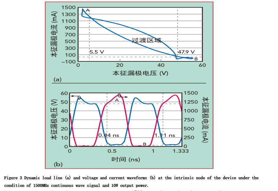
waveforms show that at a frequency of 1500MHz, the peak voltage in the power amplifier is less than 60 volts, and the peak current is less than 1500 mA, which is all within the rated operating range of the device. What's more remarkable is that in terms of efficiency, due to the near-ideal Class F working state, the current waveform after half-wave rectification and the voltage waveform form a phase difference of exactly 180 degrees. There is only a minimal voltage/current overlap area. Using DLL analysis, three regions can be defined: area A (Vmin and Imax), area B (Vmax and Imin), and transition area. In a duty cycle, the waveform stays in zone or B for 63.8% of the time, and only 36.2%
RFPA verification
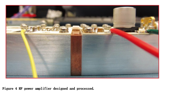
To verify this method's effectiveness, RFPA was fabricated on a 20-mil Rogers 4350B board (εr=3.48). The circuit consists of three parts mounted on the fixture, including the source matching network (INMAT), the load matching network (OUTMAT), and the central section made of copper for mounting transistor devices (see Figure 4). The source of the device is fixed by welding.
Passive measurement
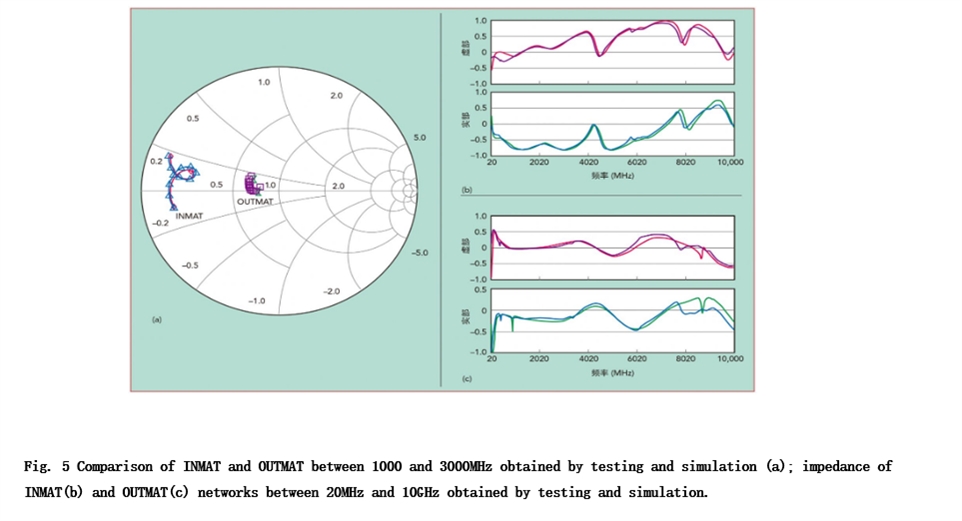
Before the final assembly, the impedances of the input matching network INMAT and the output matching network OUTMAT saw at the pin end of the transistor are measured so that the modeled and measured data can be compared. The measured data shows that the model impedance from 1000MHz to 3000MHz is very consistent with the measured data (see Figure 5a). The INMAT and OUTMAT on a broader frequency band from 20MHz to 10GHz were measured, and the results still show that the model and the measured impedance are very consistent (see Figure 5b and Figure 5c). By adopting a modular three-piece fixture, the transistor device's impedance can be directly and accurately measured, thereby avoiding the use of poorly mechanical probes and avoiding the introduction of parasitic electrical parameters, especially the parasitic inductance introduced at the detection point. The form realized by the fixture is not the version of the radio frequency amplifier when it is finally produced but an essential step in the design process, which can help reduce the uncertainty of each design stage.
Small signal measurement
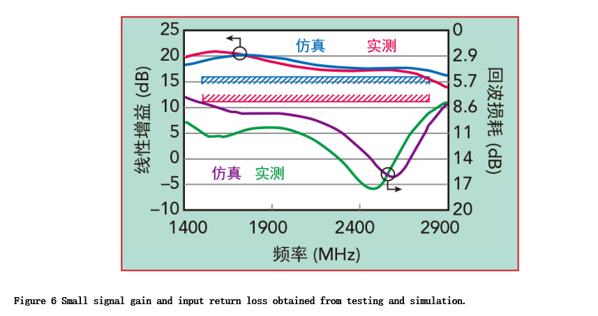
Start measuring with the small-signal gain under the conditions of drain bias voltage Vds= +28V and Idq=90mA. The gain and impedance matching of the measurement and simulation are closely related (see Figure 6). It can be seen in the figure that the small-signal gain is greater than 16dB over the entire operating frequency band, and the input return loss is more significant than 7.5dB. The amplifier can maintain stable operation under common actual stability test conditions, such as changing the drain voltage and using an external impedance tuner to change the source impedance seen by the amplifier.
Large signal measurement
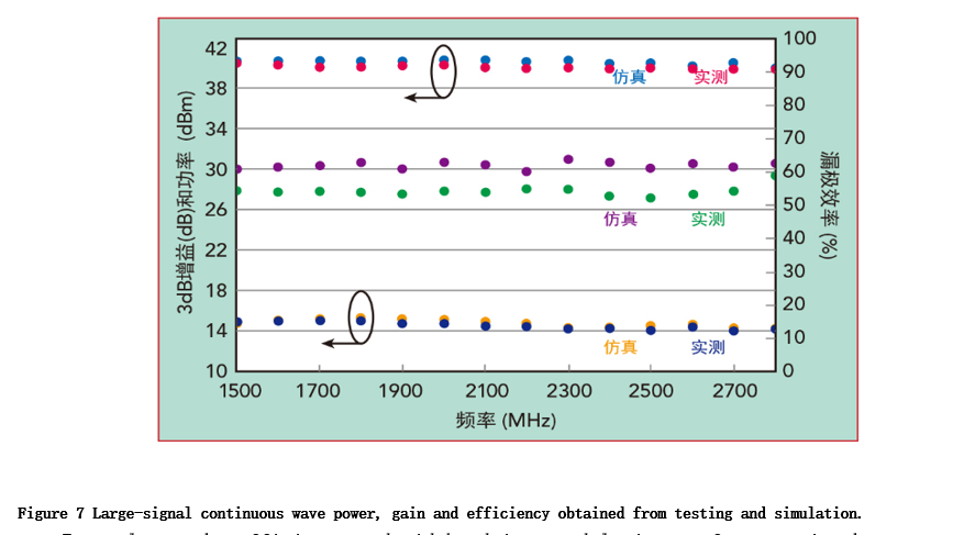
The working conditions of drain bias voltage Vds= +28V and Idq=90mA are used in the large-signal measurement. The continuous wave signal source is fed to the RF power amplifier through a drive amplifier. Any non-linear compression that may be introduced by the drive amplifier is corrected in the RF input and output power measurement. Power gain, drain efficiency, and power delivered to the load are all measured at the 3dB compression point. The simulation results show that the maximum P3dB (3dB compression point) is 41dBm, the maximum drain efficiency is 63.2%, and the maximum gain is 16.4dB. The measurement results show that P3dB is 40.6dBm, the maximum drain efficiency is 59.1%, and the maximum gain is 15.7dB (see Figure 7). The RF power amplifier provides more than 10 watts of output power in the frequency range of 1300MHz to up to 2900MHz, thereby expanding the fractional bandwidth to 76.2%.
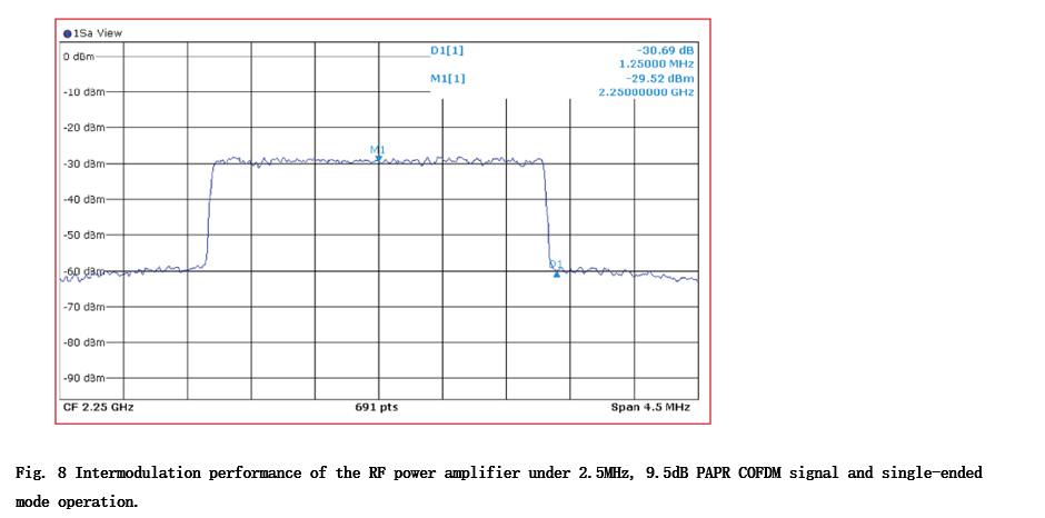
To evaluate the efficiency and sideband intermodulation performance in the output power fallback mode, a COFDM signal with 9.5dB PAPR (peak-to-average power ratio) and a 2.5MHz channel bandwidth were used for testing in the 2.0 to 2.5GHz frequency band. When used as a single-ended amplifier with 34.5dBm output power, the average efficiency is 34% to 35.9%. The measured intermodulation linearity at ±1.25MHz on both sides of the center frequency is 30dBc (see Figure 8). Similar results can also be obtained for testing using WCDMA test signals with PAPR=7.8dB in the 1.805GHz to 1.88GHz frequency band.
A balanced operating mode version of the RF power amplifier is also being manufactured. A non-ideal bridge is used in this design. The simulation reaches 37dBm power, with an average efficiency of about 34% and linearity of about 30dBc at the center frequency ±1.25MHz. Linearization techniques such as digital predistortion or envelope tracking can be used to improve linearity further. Due to the high efficiency achieved near the signal peak, the amplifier works in a more significant peak compression state to work with a higher relative power in the entire dynamic range. Therefore, efficiency and linearity are improved even when using high PAPR signals.
Completion
This article proposes a design method for broadband, linear, and high-efficiency RFPA, which minimizes uncertainty to achieve success in the first round of design. The method includes four design stages: using qualitative and quantitative analysis methods to select suitable devices, using load and source pulling technology to optimize the design of load and source impedance matching networks, and passive network synthesis including EM verification and use of internal intrinsic nodes Waveform engineering of voltage and current a proven and systematic method of designing the entire RF power amplifier is obtained.
This article also demonstrates a measurement technique using a three-piece fixture, which can test the characteristics of the source and load impedance network made so that the impedance connected to the transistor's input and output terminals can be simulated and tested. A comprehensive method of the passive network using SRFT technology combined with analysis of mismatch loss and conversion power gain is also given to obtain a relatively simple broadband matching network.


