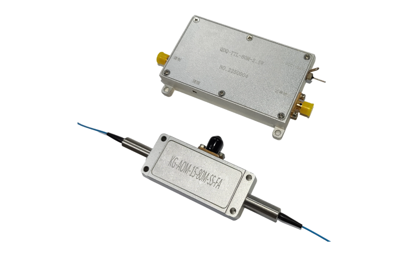
Nanolaser is a kind of micro and nano device which is made of nanomaterials such as nanowire as a resonator and can emit laser under photoexcitation or electrical excitation. The size of this laser is often only hundreds of microns or even tens of microns, and the diameter is up to the nanometer order, which is an important part of the future thin film display, integrated optics and other fields.
Classification of nanolaser:
1. Nanowire laser
In 2001, researchers at the University of California, Berkeley, in the United States, created the world's smallest laser - nanolasers - on the nanooptic wire only one-thousandth of the length of a human hair. This laser not only emits ultraviolet lasers, but can also be tuned to emit lasers ranging from blue to deep ultraviolet. The researchers used a standard technique called oriented epiphytation to create the laser from pure zinc oxide crystals. They first "cultured" nanowires, that is, formed on a gold layer with a diameter of 20nm to 150nm and a length of 10,000 nm pure zinc oxide wires. Then, when the researchers activated the pure zinc oxide crystals in the nanowires with another laser under the greenhouse, the pure zinc oxide crystals emitted a laser with a wavelength of only 17nm. Such nanolasers could eventually be used to identify chemicals and improve the information storage capacity of computer disks and photonic computers.
2. Ultraviolet nanolaser
Following the advent of micro-lasers, micro-disk lasers, micro-ring lasers, and quantum avalanche lasers, chemist Yang Peidong and his colleagues at the University of California, Berkeley, made room temperature nanolasers. This zinc oxide nanolaser can emit a laser with a linewidth of less than 0.3nm and a wavelength of 385nm under light excitation, which is considered to be the smallest laser in the world and one of the first practical devices manufactured using nanotechnology. In the initial stage of development, the researchers predicted that this ZnO nanolaser is easy to manufacture, high brightness, small size, and the performance is equal to or even better than GaN blue lasers. Because of the ability to make high-density nanowire arrays, ZnO nanolasers can enter many applications that are not possible with today's GaAs devices. In order to grow such lasers, ZnO nanowire is synthesized by gas transport method which catalyzes epitaxial crystal growth. First, the sapphire substrate is coated with a layer of 1 nm~3.5nm thick gold film, and then put it on an alumina boat, the material and the substrate are heated to 880 ° C ~905 ° C in the ammonia flow to produce Zn steam, and then the Zn steam is transported to the substrate. Nanowires of 2μm~10μm with hexagonal cross-sectional area were generated in the growth process of 2min~10min. The researchers found that ZnO nanowire forms a natural laser cavity with a diameter of 20nm to 150nm, and most (95%) of its diameter is 70nm to 100nm. To study stimulated emission of the nanowires, the researchers optically pumped the sample in a greenhouse with the fourth harmonic output of a Nd:YAG laser (266nm wavelength, 3ns pulse width). During the evolution of the emission spectrum, the light is lamed with the increase of the pump power. When the lasing exceeds the threshold of ZnO nanowire (about 40kW/cm), the highest point will appear in the emission spectrum. The line width of these highest points is less than 0.3nm, which is more than 1/50 less than the line width from the emission vertex below the threshold. These narrow linewidths and rapid increases in emission intensity led the researchers to conclude that stimulated emission does indeed occur in these nanowires. Therefore, this nanowire array can act as a natural resonator and thus become an ideal micro laser source. The researchers believe that this short-wavelength nanolaser can be used in the fields of optical computing, information storage and nanoanalyzer.
3. Quantum well lasers
Before and after 2010, the line width etched on the semiconductor chip will reach 100nm or less, and there will be only a few electrons moving in the circuit, and the increase and decrease of an electron will have a great impact on the operation of the circuit. To solve this problem, quantum well lasers were born. In quantum mechanics, a potential field that constrains the motion of electrons and quantizes them is called a quantum well. This quantum constraint is used to form quantum energy levels in the active layer of the semiconductor laser, so that the electronic transition between the energy levels dominates the excited radiation of the laser, which is a quantum well laser. There are two types of quantum well lasers: quantum line lasers and quantum dot lasers.
① Quantum line laser
Scientists have developed quantum wire lasers that are 1,000 times more powerful than traditional lasers, taking a big step toward creating faster computers and communication devices. The laser, which can increase the speed of audio, video, Internet and other forms of communication over fiber-optic networks, was developed by scientists at Yale University, Lucent Technologies Bell LABS in New Jersey and the Max Planck Institute for Physics in Dresden, Germany. These higher-power lasers would reduce the need for expensive Repeaters, which are installed every 80km (50 miles) along the communication line, again producing laser pulses that are less intense as they travel through the fiber (Repeaters).


